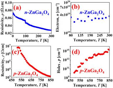
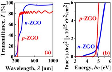
In this international joint research collaboration, Prof. Ray-Hua Horng of National Yang Ming Chiao Tung University gathered domestic professors to collaborate with Professor Chikoidzeof Paris-Saclay University. They published that both n-type and p-type thin layers exhibit high transparency >80% in 360–1000 nm wavelength range and energy gap values of 4.9 eV and 4.8 eV, respectively. The p-ZnGa2O4 films have the mobility of 7-10 cm2V-1s-1 at high temperatures (500-850 K). The electrical resistivity is 1.3 × 10³ Ω cm and has a hole concentration of p = 1.6 × 1015 cm-3 at 850 K. In contrast, the n-ZnGa2O4 film has a mobility of 5.3 cm2V-1S-1 at 300 K. It has a lower resistivity than p-ZnGa2O4: 3.2 × 10⁻² Ω cm and an electron concentration of n = 3.7 × 1019 cm-3.

These experimental facts raise up the immediate question of which the origin of the conductivity is and challenge our general view of ZnGa2O4 being a typical insulator representative. Here, based on complementary structural, chemical, optical and electrical transport measurements, we conclude that the origin of high room temperature n-type conductivity (∼3.2 × 10⁻² Ω cm at room temperature) is related to the “self-impurity” band located Ev+ ∼3.4 eV from the valence band edge. This band is a consequence of the Zn–O orbital’s hybridization in Zn-rich and O-deficient ZnGa2O4 material. On the other hand, hole conductivity in p-ZnGa2O4 is achieved thanks to ZnGa antisite defects. This national research collaboration further evidence of outstanding prospects of ZnGa2O4 material for extending the frontiers of solid-state energy optoelectronics.


